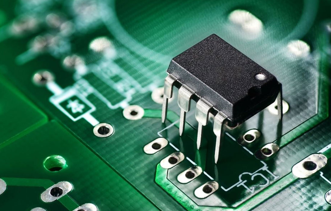
Through Hole PCB Assembly
- Home
- Through Hole PCB Assembly

Through Hole PCB Assembly
OEAS is a leading provider of Through Hole PCB Assembly services, renowned for its unmatched expertise and precision in electronic manufacturing. Our state-of-the-art facilities guarantee that every component is carefully positioned and soldered to precise specifications, ensuring the production of high-quality and reliable circuit boards.
For companies in search of trusted Through Hole PCB Assembly services, OEAS emerges as a premier partner. We are adept at managing complex assembly processes and utilizing cutting-edge technologies to adhere to rigorous industry standards. Our committed team conducts comprehensive quality checks at every phase of Through Hole PCB Assembly, from the initial design validation to the final inspection of the product.
Benefits of Through-Hole Assembly
Thermal Profiling
This is used to discover the temperature profile that works best for the through hole PCB and to point out defects such as insufficient solder, misaligned components, marginal joints and more.
Flying Probe Testing
This is particularly used in cases of low volume and highly complex assemblies helps in detecting missing components as well as to validate the component placement.
ICI Testing
ICT (In-Circuit Testing) is extensively used for high volume production; it is extremely efficient in detecting parametric failures, PCB layout-related faults, and component failures.
Functional Testing
Used to authenticate board operations and behavior, functional testing helps to detect faulty component values, functional and parametric failures.
Through Hole PCB Testing Protocols Include
Thermal Profiling
Visual Inspection
In-Circuit Testing (ICT)
Functional Testing
Recommended Services
Recommended Services
ORDER YOUR PCB NOW
Innovating Circuits, Empowering Futures.
